board layout (wsb)
After designing both boards, it was time for layout. I really have to hand it to my teammate Evan here. He's never laid out a board before, so I sat with him throughout the process, giving little hints here and there and he had no trouble routing the CCU board. For his board, we decided to go two layer, since the number of components was much smaller and there wasn't any circuitry that would be affected by poor power supply routing. For the sensor interface board, I decided to do a four layer layout. The extra layers really helped speed up the process (as I didn't have to worry too hard about power or ground connections) and helped me make the board pretty dense.
Here's what Eagle gave me when first generating the board file. This consumed me for about two weeks.

I actually really missed being constrained to a physical size. With the business card board, I knew that I wanted it to be a certain dimension. In this case, the dimension of the board was just whatever I could make it work out to. I basically started in a corner, decided that I wanted all of the connectors on a single edge of the board, and went from there, stacking things in as I could. Before I did any layout, I grouped all of the components together with their nearest logical neighbors on the schematic. This meant I could route bits in little sections and then bring them into the board as a group. Here are some progress photos.


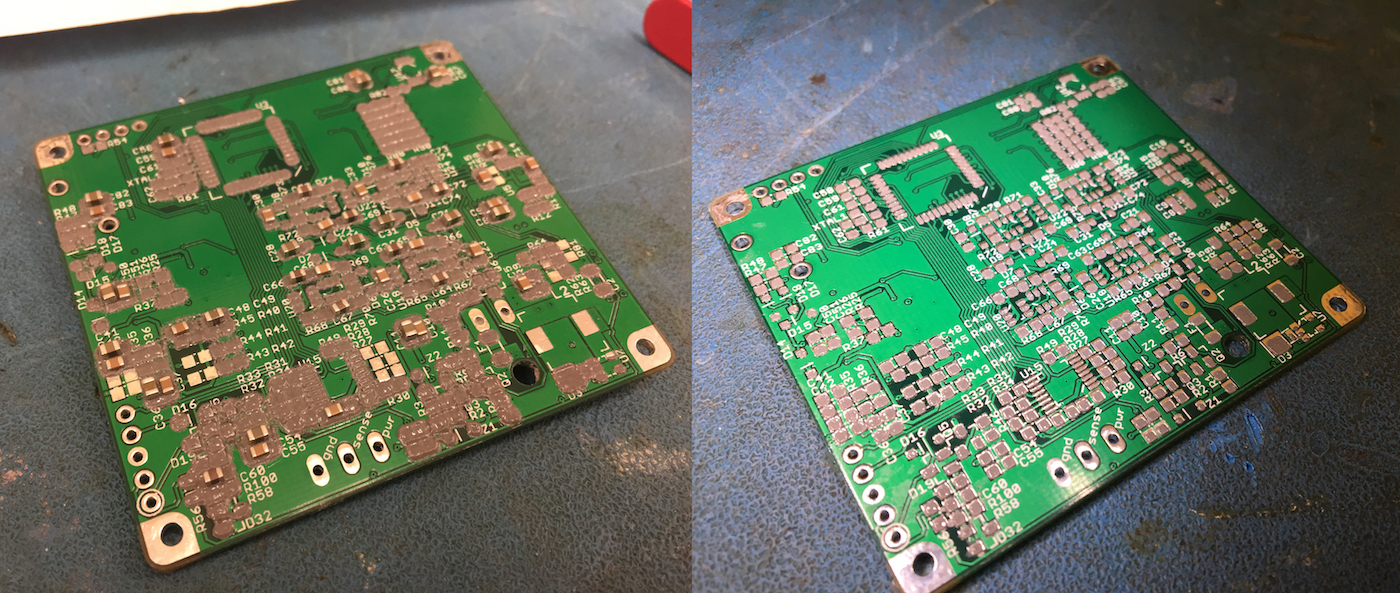
Here's the finished layout. I ended up fitting 400 parts in just under a 2.5 inch square, which I was quite proud of.


Throughout the layout process, I threw away some of the connectors I had on the board. I originally brought all of the sensor supply voltages out to a connector, but I didn't see much purpose in it after thinking about it for a while. I also removed the DC power jack and kept only the one power connector. I also removed a lot of test points, a decision I sort of regretted while debugging the board.
sending the boards to fab
At this point, we had only four weeks or so before the expo, so I was in full crunch-mode. What terrified me was waiting for the boards to come in the mail. OshPark has a rush service for two layer boards, but doesn't have the same option for four layer boards. We went with the rush service from OshPark for the two-layer CCU board, and then I sent the WSB boards to PCB minions at the recommendation of the senior design lab manager (who handles all of the procurement for the teams). I wanted to go with PCB Zone, but unfortunately the senior design ordering guidelines prohibit the use of PayPal, which was the only method of payment available on their website.

While I was waiting on the boards, I ordered some stencils from OSH Stencils.

ordering the parts
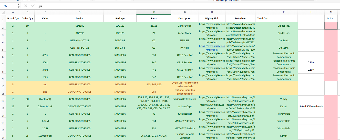
This was a huge effort. We manually combined the auto-generated BOMs from each board, as each shared a good amount of parts. What further complicated the ordering process was parts that had various qualifiers at the end that I didn't specify in the packages I made for the schematic library. I ended up going through each page of the schematic, covering each part with a rectangle when I had confirmed that it was in the BOM and that the value and link to Digikey was correct. I added ordering margin to each part to ensure we had enough if we messed up a few.
Once the spreadsheet was done, actually assembling a Digikey cart was another hurdle. I added the parts one by one, double checking the quantity in each line item. After each part was added to the cart, I colored a square red in the spreadsheet to confirm that I had actually placed the parts into the cart.
assembling the boards
Assembling the boards took a solid week of 12+ hour days in the lab with my group. While I had worked mostly alone on the design of the sensor boards, and with only Evan on the design of the central control board, the entire team came together and really helped get these things together and working.
I realized almost immediately that I had made an error in ordering the stencils. There was an incredible amount of bleeding, making the solder paste look more like a contiguous blob rather than distinct rectangles. I realized I forgot to shrink the cream layer in the design rules inside eagle. This meant that the holes in the stencil were the identical in size as the pads. I reordered the stencils, but in the meantime we made it work. You can see the difference below in the two different stencils, old on the left, new on the right.
I made this jig out of some pieces of acrylic that were laying around to hold the board off the table while the solder paste was applied to the back side of the board. Pictured are Evan's boards from Oshpark.

The first bit of the first board took a huge amount of time. For every component I placed, I looked in the board in Eagle, right clicked to get its information, found the component in a box of 200 other bags, took one component out, placed it, ad nasuem. After a few hours of this, I printed out the board and went through and labeled every component with a part number or a value. This way I could take out a capacitor, quickly look around the board for how many others there were, and then place all of them at the same time.

It took a long time, but the boards started to come together, and as my team became more confident in assembling the boards, I switched to working on board bringup of the sensor boards. My teammate Ethan had already been writing a lot of code for the CCU (since we based it around the MBED, a lot of it was breadboard-able), and he switched to ensuring the one CCU board we assembled was fully functioning.


board software
I don't think I'm going to go much into the particulars (line by line) of the code I wrote for the sensor boards here. Though I will say I am very proud of how clean the code was in the time crunch situation I wrote it in. I abstracted away almost all of the hardware and register settings into small libraries. I started with the SPI peripheral, and then built on top of that to abstract away the I/O expanders and the A/D converter. Eventually I abstracted away most of the analog sensor front end to the point where I could set a voltage division ratio by calling: afe_set_voltage_division_ratio(AFE_DIVIDER_RATIO_OPEN);
Getting the boards to work was quite a task. I spent a lot of hours with them on my desk in this configuration:

The most exciting moment was probably when I brought my code that I had written for the sensor interface boards together with the software that Evan had been writing for the control board. Here's the first time we got a voltage reading to transmit over to the central board.
Here's really the first time our design goal was completed. In this video the sensor (in this case a potentiometer's wiper voltage) is being read, transmitted wirelessly to the central control board, where it is relaying it to an OBD-II dongle over the CAN bus, which relays the information to a smartphone.
design issues, lessons learned
There's lots of these. This was the most complicated electronics project I've ever worked on, and while our solution was somewhat complicated by me in a desire to make a generic solution, I am happy I made it hard on myself since I learned so much in the process. However, my design was not without fault, and I caused a lot of headaches with some simple mistakes, so I thought I'd cover those here.
part/library management
I should have added a lot more metadata to each component to make the ordering process easier. We burned a lot of time going back over parts that had been picked weeks before trying to figure out which one was meant to be ordered. Some parts made this particularly difficult. A few TI parts are identical except for a different letter at the end of the part name which signifies a newer or older part, even though both parts may still be actively produced. I'm not sure this can be remedied for every part without spending a large amount of time. At past jobs, each capacitor and resistor value is a different package in the library, each associated with a part number from the manufacturer. I could have done this for the larger parts though.
incorrect relay package
This is a simple one, I didn't realize the part in the relay datasheet which noted the pinout was as seen from bottom. As the relay had two poles, symmetric down the middle of the package. However, it does matter the polarity in which the relay is driven, if the primary side is energized in the wrong polarity it simply reinforces the resting state of the switch. To fix this, we soldered a few relays upside down with little pieces of wire draping down and connecting to the pads.
incorrect calibration logic
The relay was useless anyway, as I didn't fully think through the calibration idea that I had. If even the lowest current source is enabled when the sensor is disconnected, and I have a 0 ohm jumper as one of the tails of the voltage divider (to ground), then the current still passes through a fixed 499k resistor. At a microamp of current this creates a half a volt. This would work to calibrate the lowest current source, but as soon as the next order of magnitude of current is selected (10 microamps) the output jumps to a half of a volt, which is outside the input range of the A/D converter. So, this means only the lowest current source can be calibrated.
To fix this a smaller resistor would have to be picked as the top of the voltage divider, but this has other issues, such as loading down the output of the sensor. So more work would have to be done here for this to be a great idea.
bad voltage buffer buffer design
If you'll note in this schematic, if none of the open drain buffers are enabled, then the noninverting input of the voltage buffer is left floating. In the early stages of testing the board kept browning out in cycles after the boost converter was enabled, which brings up the 5V rail that powers the analog circuitry on this page. We spent a lot of time tracking down soldering issues with the boost converter before I realized that when no voltage division was enabled, and no sensor was connected, there was nothing pinning down that opamp input. The input capacitance of the opamp charged up over time, before it was buffering around 3.3V, which is then clamped to the 3.3V rail without any current limitation through D14.
I solved this by making sure in software that the boost converter wasn't turned on until at least one voltage divider was enabled or a sensor was connected to the board. A real fix would be adding some current limiting resistors to the clamping diodes D14 and D15.
backwards mosfet
I couldn't get the current source to work at first, and I scratched my head a bit until measuring the output of OP1A and realizing it was pegged at the rail, keeping the MOSFET fully on. I couldn't figure this out until I looked back at the schematic and realized that the drain and source of the MOSFET are in the opposite positions as needed. With the configuration shown in the schematic, as soon as the mux connects one of the resistors to the 5V rail the body diode is forward biased which then turns the MOSFET on. My quick fix for this was flipping the MOSFET upside down and rotating it into place on the board, bridging the gaps to the pins with some blobs of solder. Not pretty, but it made my current source work.
I/O expander bringup
I couldn't for the life of me get any I/O expanders to respond at first. I kept noticing very weird behavior on the bus. I hunted down shorts on the board for a while, which made the behavior different, but didn't fix the problem. It wasn't until I noticed in an app note for the expander that the addressing feature is disabled until a register is set. Until the register is set, all I/O expanders respond as if their address pins are tied to ground. So one of the first steps when the board turns on is to communicate to address 0, 0 and enable addressing, after which each expander only responds to its specific address.
12V voltage divider
I really wanted to show that the sleep-mode that I had designed into the board was actually low power, except when I put the board into a sleep state by disabling the buck converter and putting the microcontroller into a sleep mode I was still seeing over a milliamp of current consumption on the 12V input. At first I thought it was an oscillator issue, so I spent a while making sure the microcontroller was switching from the external crystal oscillator to the low-power internal oscillator. It didn't seem likely that an oscillator was consuming an entire milliamp, and that was in fact the case.
It took me a bit of looking over the schematic to find the voltage divider I had placed to measure the battery voltage. Sitting between the 12V rail and ground was a 10k and 787 ohm resistor forming a divider. As soon as I removed the 10k resistor from the board (disabling the battery voltage measurement feature) the current was well into the microamps, and I was happy.
poor component selection
I tried to keep most of the components in an SOIC or TQFP package to keep the pins exposed, but for some reason I chose the most needlessly tiny parts for some of the most critical components, namely the buck converter and the low-current sleep power supply. These things were a complete pain to get soldered correctly with the tools we had at our disposal. The buck converter was especially tricky with it's tiny unexposed pads.
have margin, but not too much
One example here would be the sensor supply linear regulators. These things are huge, I think they have a maximum rated current of about 1.5A. One of the specifications for the sensors we had was not consuming more than 20mA. I could have picked a much smaller regulator.
overdesign
I mean, I'll be honest, all of the things this board did probably could have been done with much simpler hardware targeting the specific sensors, but generic-ness was a part of the design goals, so some of the complexity was necessary. However, the analog front end ended up being much more precise than the A/D converter could resolve and most of the sensors that we were interfacing with are low precision anyway, so the extra complexity probably was not needed. Taking a step back could have been useful, to determine what margins and accuracy was really needed (do I really need 0.1% resistors?).
results
In the end (the night before the expo), we got a wireless board wired up in my car to my existing sensor, transmitting oil pressure data to the central board. On our table at the expo we also had a resistive sensor and a pulse frequency sensor (a flow-meter measuring water flow in a jig that my teammate Kyle built), showing that we had gotten all three sensors working. All of the data was transmitted to a laptop using a Bluetooth OBD-II dongle. Here are some photos from the expo.


The judges seemed fairly impressed with our project, though I think a lot was lost on the non-EE judges. From first glance, the results of our project appear very simple. Stepping on the gas, increasing oil pressure, just makes a little dial on the computer screen turn. It's not really that interesting of a thing until you realize how much work went into the project, and understand how the solution can interface with any number of different sensors.
I think this is a great first start, and actually something that I would be interested in developing further with my team members. I can think of a lot of improvements to the hardware and software that would make it much more usable, but I think we'll be preoccupied with celebrating finishing our undergraduate degrees for a while.